Instructions and Processors in MIPS
Three instructions formats:
![MIPS instruction format [18]. | Download Scientific Diagram](https://osh.fducslg.com/notes/~gitbook/image?url=https%3A%2F%2Fwww.researchgate.net%2Fpublication%2F220239180%2Ffigure%2Ffig1%2FAS%3A349293304139776%401460289421176%2FMIPS-instruction-format-18.png&width=768&dpr=3&quality=100&sign=dffe3a5f&sv=2)
R-Type Instructions:

J-Type Instructions:

I-Type Instructions:

Note that the target address of
beqisPC + 4 + SignExt(imm16) * 4.
Exceptions
Exception state is kept in "coprocessor 0":
Use
mfc0to read contents of these registers.Every register is 32 bits, but may be only partially defined.
BadVAddr (register 8):
Register contained memory address at which memory reference occurred.
Status (register 12):
Interrupt mask and enable bits.
Cause (register 13):
The cause of the exception.
Bits 5 to 2 of this register encodes the exception type (e.g., undefined instruction=10 and arithmetic overflow=12).
EPC (register 14):
Address of the affected instruction (register 14 of coprocessor 0).
Control signals to write BadVAddr, Status, Cause, and EPC:
Be able to write exception address into PC (8000 0080_hex).
May have to undo PC = PC + 4, since we want EPC to point to offending instruction (not its successor): PC = PC - 4.
Single-cycle MIPS Processor
Storage Elements
The clock input (CLK) is a factor only during write operation. During read operation, the storage elements (register file/idealized memory) behave as a combinational logic block. The output data will be valid after "access time".
The clocking methodology of the storage elements:

D value must be held stable during the decision window for some period before (setup time) and after (hold time) the clock edge.
Clock-to-Q is the time for the output value Q to be the same with the input value D.
Hold Time should > Clock-to-Q
【TODO】
Datapath

Critical Path (Load Operation) = PC's CLK-to-Q + InstMem's Access Time + RegFile’s Access Time + ALU to Perform a 32-bit Add + Data Memory Access Time + Setup Time for RegFile Write + Clock Skew.
Control Signals
nPC_MUX_sel
0 => PC <- PC + 4; 1 => PC <- PC + 4 + SignExt(Im16)
ExtOp
Zero-extension or sign-extension
ALUsrc
0 => regB; 1 => imm
ALUctr
add, sub or or.
MemWr
Write to the memory if asserted.
MemtoReg
0 => ALU; 1 => Mem
RegDst
0 => rt; 1 => rd
RegWr
Write to the register if asserted.
The data path also yields Zero signal if the output of ALU is 0.
Note that in real implementation, the next PC is determined by the combination of
Jump,BranchandZerosignals rather than the simplifiednPC_MUX_selhere.
A Summary of the Control Signals:

Local Decoding: A separate decoder will be used for the main control signals and the ALU control. This approach is sometimes called local decoding. Its main advantage is in reducing the size of the main controller. The ALUctr determination is a two-stage process based on the func and op fields:

For instance, R-type operations like add, sub, etc., use "R-type" as the symbolic representation in the ALUop field and are further defined by the func field. For other instruction types, the ALU's behavior is directly dictated by the op field.
The decoding for R-type instructions is detailed as follows:
func[5:0]
Instruction Operation
100000
add
100010
subtract
100100
and
100101
or
101010
set-on-less-than
Based on the encoding specification of op and func, we can derive that:
ALUctr[2]=!ALUop[2] & ALUop[0] + ALUop[2] & !func[2] & func[1] & !func[0]ALUctr[1]=!ALUop[2] & !ALUop[1] + ALUop[2] & !func[2] & !func[0]ALUctr0=!ALUop[2] & ALUop[1] + ALUop[2] & !func[3] & func[2] & !func[1] & func[0] + ALUop[2] & func[3] & !func[2] & func[1] & !func[0]
Multi-cycle MIPS Processor
Motivation
Long cycle time: all instructions take as much time as the critical path takes.
Real memory is not as nice as our idealized memory: we cannot always get the job done in one (short) cycle.
Two memories (IM, DM) and three adders (ALU, PC and Branch): we want the design to be smaller.
The idea of multi-cycle design is to do same work in a number of fast cycles rather than the slow one.

The FSM of the Main Controller

S0
PC = PC + 4 and store the instruction to IR.
S1
Decode the instruction (i.e. op, func, rs, rt, rd, imm) Note that the target address of branch instructions can be computed at the end this state if the operation is branch, which saves one cycle.
S2
If the operation is sw or lw, calculate the address based on rs and imm. The calculated address is stored in ALUOut.
S3
If OP is lw, the IorD is asserted. Read the memory and store the result in DR.
S4
Memory write back to register from DR. RegDst=0 stands for rt while MemtoReg=1 stands for DR.
S5
Write to the address specified by the ALUOut.
...
...
Pipelining
Suppose we execute 100 instructions.
For a single-cycle machine, it takes 45 ns/cycle x 1 CPI x 100 inst = 4500 ns
For a multi-cycle machine, it takes 10 ns/cycle x 4.1 CPI (due to inst mix) x 100 inst = 4100 ns
For a idealized 5-stage pipelined machine, it takes 10 ns/cycle x (1 CPI x 100 inst + 4 cycle drain) = 1040 ns.

Performance Metrics
The maximum throughput of a pipeline is constrained by its slowest stage, often referred to as the bottleneck. This can be expressed mathematically as:
To complete n tasks across m stages, where each stage takes the same amount of time, the total time required is:
Therefore, the throughput is:
To approximate the maximum throughput, set m=1 or let n→∞. This minimizes the filling and draining phases, enhancing the efficiency of running the pipeline.
Two common approaches for improving the maximum throughput:
Parallelize the bottleneck.
Split the bottleneck.
Speedup: the ratio of pipelining speedup to equivalent sequential time.
Efficiency: the ratio of the spatiotemporal region of the sequential time to the region of pipelining:
Tradeoff
Where G is the price of non-pipeline processor, k is the pipeline stages and L is the price of latch.
Where T is the latency of non-pipeline processor, S is the latency of latch.

Hazards
Structural hazards
Attempt to use the same resource two different ways at the same time.
Consider a scenario where both R-type and load instructions are processed in a pipeline. R-type instructions, which lack a Write Register (WR) stage, complete in four stages. In contrast, load instructions require all five stages. This setup can lead to structural conflicts, as illustrated below:

Observation 1: every functional unit should be utilized only once by a instruction.
Observation 2: every functional unit should be utilized only at the same stage for all instructions.
Solution 1: insert “bubble” into the pipeline. Drawbacks: (1) the control logic can be complex. (2) lose instruction fetch and issue opportunity.

Solution 2: delay R-type’s write by one cycle. Mem stage of R is a NOOP stage: nothing is being done.

Control hazards
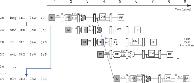
Solution 1: stall the pipeline until the branch decision is made (i.e., PCSrc is computed). Because the decision is made in the Memory stage, the pipeline would have to be stalled for three cycles at every branch. For J-type instructions, the decision can be made at the end of the RF stage, which can save us a cycle.
Solution 2: predict the next instruction. 0 lost cycles per branch instruction if right, 1 if wrong (right 50% of time). Assume that the accuracy of predition is 90%, the average CPI of branch is 0.9×1+0.1×2=1.1. Assume that branch accounts for 20% of the instructions, the total CPI might then be 1.1×0.2+1×0.8=1.02.
Solution 3: delayed branch. We redefine branch behavior (takes place after next instruction).
Delayed jump / branch technique: the compiler fills the delay slot(s) with instructions that are in logical program order before the branch.The moved instructions within the slots are executed regardless of the branch outcome.
The probability of:
Moving one instruction into the delay slot is greater than 60%
Moving two instructions is 20%
Moving three instructions is less than 10%.
The delayed branching was a popular technique in the first generations of scalar RISC processors, e.g. IBM 801, MIPS, RISC I, SPARC.
In superscalar processors, the delayed branch technique complicates the instruction issue logic and the implementation of precise interrupts. However, due to compatibility reasons it is still often in the lSA of some of today's microprocessors, as e.g. SPARC- or MIPS-based processors.
Data hazards
RAW (read after write)
WAW (write after write)

WAR (write after read)

Solution 1: forwarding or bypassing can address most data hazards. However, for load instructions, which fetch data that subsequent instructions depend on, forwarding isn't feasible. In such cases, we must implement delays or stalls for instructions that depend on the load operations.

Name Dependencies
A name dependence occurs when two instructions use the same register or memory location, called a name, but there is no flow of data between the instructions associated with that name.
Write after Read (WAR/Anti/False/Name)
An antidependence between instruction i instruction j occurs when instruction j writes a register or memory location that instruction i reads. The original ordering must be preserved to ensure that i reads the correct value.
The following code has a WAR dependence on R1.
Write after Write (WAW/Output/False/Name)
An output dependence occurs when instruction i write the same register or memory location. The ordering between the instructions must be preserved to ensure that the value finally written corresponds to instruction j.
The following code has a WAW dependence on R1.
Because a name dependence is not a true dependence, instructions involved in a name dependence can execute simultaneously or be reordered, if the name (register number or memory location) used in the instructions is changed so the instructions do not conflict.
This renaming can be more easily done for register operands, where it is called register renaming. Register renaming can be done either statically by a compiler or dynamically by the hardware.
Control Signals

Last updated